According to the IPC PCB, testing a PCB is a must for the security of the product user.
So, one thing is clear you can not launch any sort of electronic product without testing the PCB.
Now, testing a PCB is not that easy. Many manufacturers are still confused about the right testing method to adopt or are doing it wrong. Thus, the best move is to hire PCB design services. Still, just for your information, we are using a blog about PCB testing methods.
Types of PCB Testing Methods
Visual Inspection
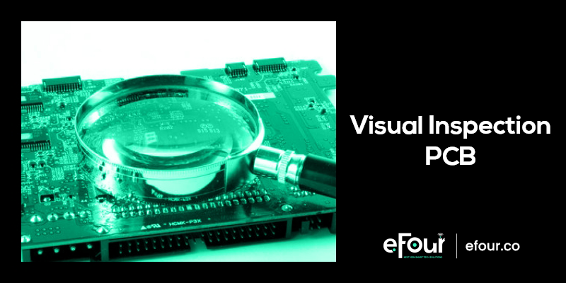
Visual inspection is one of the most basic PCB testing methods. All you need to test a PCB via the visual inspection method is a magnifying glass. As it is the simplest method, it is the first test every PCB manufacturer performs.
This method is used to test the components for their orientation, connection, design of the board, soldering, and other defects that can be detected visually.
Though it has limited coverage, it helps detect defects at an early stage, which can help avoid expenses on costly tests.
Advantages:
Disadvantages:
In-Circuit Testing (ICT)
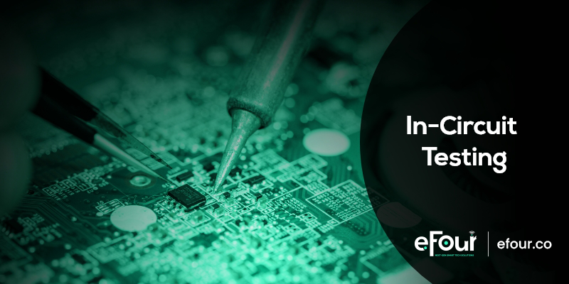
In-circuit testing is probably the one you heard the most about. It’s one of the most popular tests due to its ability to test products in large batches. As it is an automated test, manufacturers claim its accuracy to be 98%, which makes it one of the most reliable PCB tests.
It is conducted at the end of the production line before the functionality test to check if every component is placed correctly and electrically connected.
The ICT test is also known as the bed-of-nails test. Wondering why so?
The name bed-of-nails explains how the PCB is tested in this robust method. The PCB is tested by connecting probes to the test points, pre-designed in the PCB. The testing apparatus is a system of thousands of sensors and drivers which test the PCB rigorously.
Advantages:
Disadvantages:

Want to perform an In-Circuit Test on Your PCB? Contact us to get your PCB tested by professionals.
Flying Probe Testing/Fixtureless In-Circuit Test (FICT)
Flying probe testing or fixtureless in-circuit test goes one step ahead in the PCB testing methods. Unlike the ICT, FICT can test the PCB on not only the pre-defined test points but also from untended vias. Moreover, it can directly test the PCB components like diodes, capacitors, inductors, transformers, etc.
As the flying probe test does not need the fixtures like the ICT, the cost of testing goes down. The FICT is flexible enough to test different boards quickly with just a quick tweak in programming. This flexibility has made it a common testing method amongst electronics manufacturers all over the world.
Another benefit of this test is that since the probes are free to move, you do not need as many probes as you need in the ICT. You can test the same PCB with fewer probes by moving it from one testing point to another. This fact plays a significant role in bringing the cost of PCB tests down.
Advantages:
Disadvantages:
Boundary Scan Testing
The boundary scan testing method is to test integrated circuits (ICs). This method helps to test the nodes that are not easily accessible because of the compact design. The boundary test mainly covers the wire linings on the IC.
In this testing method, cells are fixed in the leads from silicon to the external pins. This way, it doesn’t need to reach all the nodes for testing. And that is the primary reason it can test PCBs with multiple layers or high density.
Advantages:
Disadvantages:
Automated Optical Inspection (AOI)
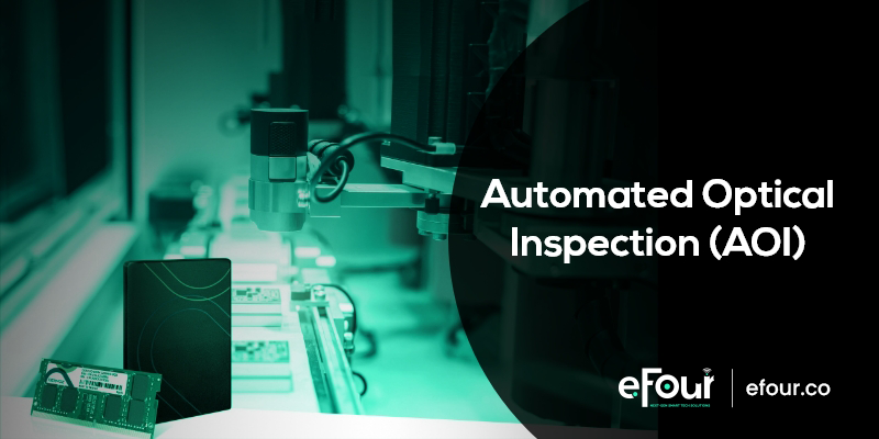
Automated Optical Inspection is the digitized version of visual inspection. This method is just more accurate and high-tech than the manual inspection PCB testing methods.
In this method, the PCB is scanned by cameras to detect mainly two types of defects which are: catastrophic failures and quality failures. Let’s see a few examples of both.
Catastrophic failures: Missing components, missing connections, broken boards, etc.
Quality failures: Improper component fixing, skewed components, or incorrect connections.
Advantages:
Disadvantages:
Burn-In Testing
The burn-in testing for PCBs is what road tests are for vehicles. The team stimulates the real-world conditions and programs as per the design. It covers all the functions the PCB has to perform using all the components.
Once the PCB has passed the test, the level is stepped up and the PCB is tested for conditions beyond the mentioned limits. This is to examine the early failures and actual load capacity.
Advantages:
Disadvantages:
X-Ray Inspection
When dealing with complex PCB designs, testing every soldering joint might not be possible because they are hidden in the layer beneath. And that’s when X-ray comes into the picture. As you might know, X-ray can take images of the layers.
Also, this test is carried out to examine the body of the components. Modern technology helps manufacturers to create 2-D as well as 3D scans of the solder joints to make them 100% defect-proof.
Advantages:
Disadvantages:
Well, the list doesn’t end here. There are many PCB tests specific to the testing requirement.
So, let’s quickly talk about a few of those.
efour provides complete PCB design services with manufacturing and testing included. So what are you waiting for?
Other Functional PCB Testing Methods
The PCB has to undergo tests for multiple reasons and functions and basically, every function can have its own separate test.
So, covering each of them is next to impossible. However, here are a few common other functional testing methods for PCBs.
Solderability test: It is to make sure surface reliability and chances of forming a strong solder joint.
Micro-sectioning analysis: Investigates defects like short circuits, opens, and other failures.
Time-domain reflectometer (TDR): Practiced to test high-frequency PCBs.
PCB contamination testing: Detects bulk ionics so that your PCB does not get contamination due to corrosion.
Peel test: Covers the strength test of the laminated board.
Conclusion
Testing PCBs is a must task that can not only get you surety about the functioning of the PCB but avoid accidents as well.
So, if you want to test your PCBs, efour is your go-to place. We are experts in high-speed PCB design services ready to provide you with a PCB that you can rely on.
FAQs
To test a new PCB you can run it through tests like