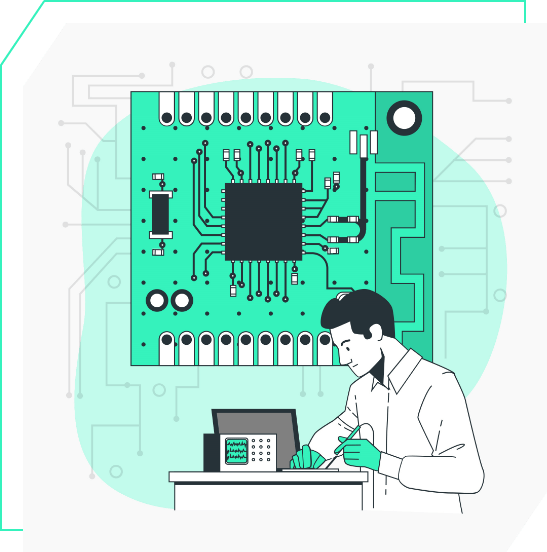
Printed Circuit Board (PCB) Design, Layout & Development Services
As a leading PCB design company, we have years of experience designing PCB layouts. Our expert PCB design engineer always ensure to provide high quality PCB Design Services. Let’s connect with us to design your own PCB now!
Leading PCB Design Company

We, at efour, are proud partners to many organizations when it comes to PCB design services. Whether you’re looking for custom PCB design from scratch, PCB layout service or a PCB design consultant to optimize your board, we’ve got you covered on all fronts.
With efour as your PCB design company, you’re getting an experienced team specializing in custom PCB design, development and layout for analogue, digital, and mixed signal boards. These boards can be employed in various fields and electronic systems.
Our PCB Design Services Capabilities:
Our PCB Design Services Offerings
We offer you across the board PCB services that take care of almost everything there is to do with PCB. You can consider us as your PCB design and layout development company who’s by your side 24/7. Here are the PCB layout design services that we offer:
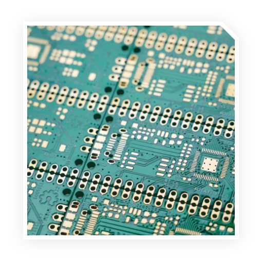
Multiple types of Printed Circuit Boards
We provide you PCB design services for various types of circuit boards. You will get custom pcb design services for each of your product requirement.
Single-Sided PCB
A single-sided PCB is the most commonly used printed circuit board. It comprises a single conductive copper layer above the substrate. Thus, all electrical components are soldered or fixed only on one side of the board while the other displays the entire etched circuit.
Single-sided printed circuit boards (PCBs) are used for essential appliances such as calculators, power supplies, LED lighting boards, FM radios, timing circuits, etc.
Doubled Sided PCB
In a double-sided PCB, a thin layer of conducting material (usually Copper) is added to the top and bottom sides of the board. These circuit boards consist of holes that allow metal parts to be connected from one side to the other.
These are employed in cell phone systems, power monitoring, amplifiers, HVAC application, UPS system, etc.
Multi-Layer PCB
PCBs consisting of at least three conductive layers fall under the ‘multi-layer PCB category. Designed in a sandwich way, these PCBs have several double-sided conductive layers divided by an equal number of insulating material sheets.
Multi-layer PCBs are commonly found in complex devices such as computers, laptops, mobile phones, tablets, medical equipment, GPS trackers, etc.
Rigid PCBs
As the name suggests, these PCBs are rigid in physical terms. They come with a solid base that cannot be twisted or folded. These PCBs usually include four layers, namely substrate layer, a copper layer, a solder mask layer, and a silkscreen layer.
Depending upon the application, these PCBs could be single-sided, double-sided or multi-layered. They’re commonly used in GPS equipment, computers, mobile phones, X-rays, heart monitors, CAT scans, MRI systems, temperature sensors, control tower instrumentation, etc.
Flex PCBs
These printed circuit boards are made of circuits and components that are arranged on a flexible substrate. They’re usually made of polyamide, PEEK (Polyether ether ketone), or a transparent conductive polyester film. They’re also regarded as ‘versatile PCBs’.
Thanks to their flexibility, they’re used in organic light-emitting diode (OLED) fabrication, LCD fabrication, flex solar cell, automotive industries, cellular telephones, cameras, etc.
Rigid-Flex PCBs
Rigid-Flex PCB combines the best of rigid and flex PCBs to give you PCBs that embody both these characteristics. In these PCBs, both rigid and flex PCBs are attached to each other. The flex PCBs are used as interconnections between rigid PCBs.
Their compactness makes them an ideal PCB in fields such as aerospace, medical, and consumer electronics.
Our Step-by-Step PCB Design Process
When it comes to custom PCB development, we pride ourselves on being an end-to-end service provider. This means we take care of everything, from writing down circuit specifications to being certified for use. You can see our step-by-step process below. This process will help help you to know how to design a pcb for your product.
Documenting Technical Specifications

While this may not be a technical design or fabrication process, documenting technical specifications is equally vital, if not more. We first sit down with our customers (physically or virtually) to know their exact requirements.
Once done, we prepare a detailed document containing all the details, including technical specifications, block diagrams, deliverables, a preliminary bill of materials (BOM) and BOM costs, tools, technologies, etc. We take the first step quite seriously as further steps depend upon it.
Schematic Design of PCB

Once we have understood the specifications, the next step is to get on the drawing board and prepare a schematic or a circuit diagram. These diagrams are prepared in designing software such as Altium, Eagle, CAD, Allegro, ExpressPCB or Multisim. As each software has its pros and cons, you can let us know if you want us to use a particular one.
Preparing PCB Layout

After importing the schematic to the PCB layout, we manually place various components on the board and wire or route them to traces. Next, we test them for their signal integrity and electrical limitations to ensure the safety of the board.
We also use software such as Eagle to make sure that the board has been designed with no errors, thus minimizing design revisions and development costs. We also offer exclusive PCB layout services to many of our clients.
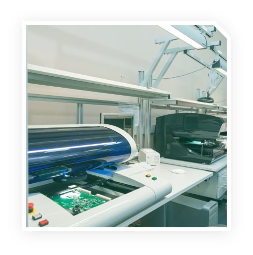
PCB fabrication

Next, we print the PCB of the schematic design producing the desired output. We finalize it to generate a film after performing DFM checks. Then we use an extremely accurate jet printer which gives a PCB with every minor detail. For PCB fabrication and assembling, we create a negative image made from a CAD software.
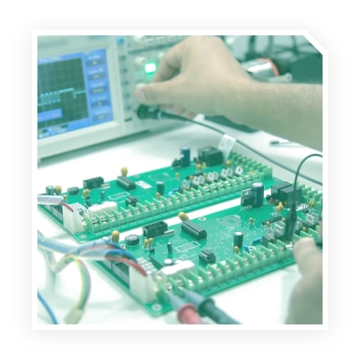
Testing & Approval

When it comes to testing Printed Circuit Board, we have a simple philosophy: no prototype should go untested. Before approving the prototype, we perform various tests, including electrical & impedance tests on the plant, followed by in-house testing. Prototypes are approved only after passing through these tests.
Hire Experienced & Certified PCB Design Engineer
Hire an experienced and highly skilled printed circuit board designer from efour. Our team of PCB designers are experienced to design various PCB as per circuit and your business requirement. Get high-quality printed circuit board designs from our certified PCB engineer.
Frequently Asked Questions
Our PCB design engineer’s team has years of experience when it comes to PCB design and layout optimization. We’ve helped many companies achieve drastic performance improvements and would love to help yours!
You can ask the PCB manufacturer or the PCB design company to sign an NDA (non-disclosure agreement) to protect your design legally.