High Speed PCB Design Services & Development Company
Top Notch High Speed PCB Manufacturing Company

We, at efour, are a high speed PCB design company with expertise in the entire PCB design process. Whether you’re looking for custom high speed PCB design services, high speed PCB layout, high speed PCB manufacturing or even hardware simulation & analysis, we stand right by you at every turn of the road.
Thanks to our competent team, years of expertise, quick turnaround time and cost-effective design, efour has become a leading high frequency pcb design company when it comes to providing world-class high-speed PCB design services. Our high-speed Printed Circuit Boards work at high speeds for applications such as FPGAs, DSPs, microprocessors, power systems and many more.
High Speed PCB Design Service Capabilities
Design Process of High-Speed PCB Layout
efour offers end-to-end PCB design & manufacturing service. From the moment we put things on paper until their certification, we do it all ourselves.
Here’s an overview of the procedure we implement:
Documenting Technical Specifications

To create any remarkable thing, you need to visualize it first. We firmly believe in this power of visualization and try to create the optimum level of documentation based on your requirements. Thus, we first sit with you to understand your end goal, budget and deadlines.
After understanding everything about your requirements and business, our team prepares an in-depth document containing all the details, including technical specifications, block diagrams, deliverables, a preliminary bill of materials (BOM) and BOM costs, tools, technologies, etc. Once done, we confirm with you to ensure that we’re on the same page.
PCB Schematic Design

After the documentation, the immediate step is to create an illustrated version of it by preparing a schematic or a circuit diagram. We use various designing software like Altium, Eagle, CAD, Allegro, ExpressPCB, Multisim, etc. We try to choose the software based on your requirements, and you can also let us know if you want to use anyone in specific.
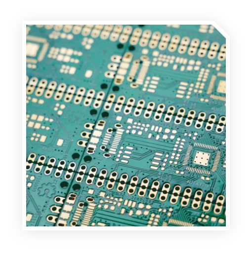
Preparing PCB Layout

Once you and our product engineering team approve the schematic design, we import the schematic design to the PCB layout, manually place various components on the board and route them to traces. This is followed by signal integrity and electrical limitation checks to ensure the board’s safety.
We further use Eagle software to weed out any errors in the board. This minimizes the revisions and development cost-time.
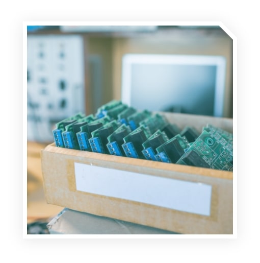
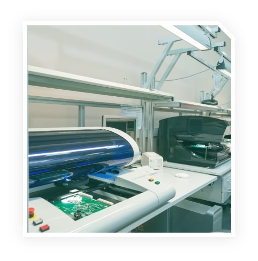
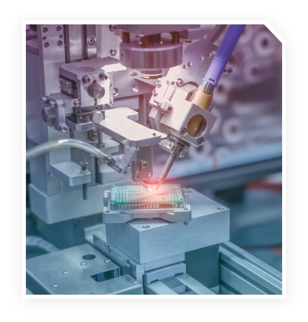
PCB fabrication

Once the layout has passed through the QA processes, we print the PCB of the schematic design that produces the desired output. This is followed by DFM checks, which generates a film. Then, a precise jet printer is employed to print a PCB to have every detail in it.
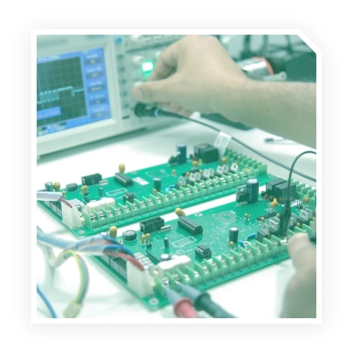
Testing & Approval

‘A product not tested is not good enough to use’ – We deeply believe in this, and that’s why we don’t leave a single stone unturned when it comes to testing PCBs. The PCBs undergo electrical & impedance tests on the plant, followed by rigorous in-house testing. Only then, we approve the prototypes.

Why Choose efour?
High-Speed PCB Layout Techniques
We employ various techniques to analyze and test the PCB while going through design and layout processes. This includes Signal Integrity analysis, Thermal analysis, Power Integrity analysis and EMI/EMC.
Signal Integrity Analysis
Signal Integrity analysis plays a crucial role for high-speed PCB designs as it impacts PCB significantly. It helps us discover and rectify parasitic capacitances and inductances of conductors, mutual induction of adjacent conductors, and circuit inconsistency. We perform IBIS model-based signal integrity analysis to do so.
Power Integrity (PI) Analysis
Power Integrity (PI) analysis allows us to simulate power distribution and thereby helping us detect circuit issues before it goes into manufacturing. The PI analysis is done through methods such as DC-Drop simulation, decoupling analysis, plane noise analysis, etc. These methods are hard to detect in a lab environment and help minimize design revisions.
Thermal Simulation & Analysis
It’s no secret that heating issues and PCB go hand in hand. At efour, we try to minimize them by thermal simulation and analysis. This includes simulation of board thermal behaviour, thermal gradient and distribution, hot spot identification, etc. These tests try to discover overheating issues and eliminate them, thereby minimizing maintenance and warranty issues.
Electromagnetic Compatibility Analysis (EMC)
Electromagnetic compatibility (EMC) is the ability of an electronic system to operate within an electromagnetic environment satisfactorily without generating intolerable EMI (electromagnetic interference) in nearby devices/systems. This is ensured by performing EMC analysis of PCBs and improving their electromagnetic compatibility.
Hire High Speed PCB Design Engineer
Hire our expert high speed PCB design engineer and take advantage of the high-quality & high frequency printed circuit board designs. Our team of PCB Designers ensure to provide high-speed board design services for electronics product development.
Frequently Asked Questions
Contrary to popular opinion, high-speed PCBs aren’t the ones operating at lower frequencies, but it is where the integrity of your signals starts to be affected by the physical characteristics of your circuit board, like your layout, packaging, layer stack-up, interconnections, etc. The amount of attention paid to these issues makes it a high-speed PCB design.
Although there’s a thin line between simple PCB design and high-speed PCB design, edge rate (also known as ‘rise time’) is a frequently used indicator of high-speed PCB design systems.
High-speed PCB design is a methodology that focuses on creating circuit board designs that are less susceptible to signal integrity, power integrity, and EMI/EMC problems. Thus, resulting in greater performance and lesser issues in the final product.
What factors should be considered while designing high-speed PCBs?
Here are the things that must be considered while designing high-speed PCBs:
Below are the main challenges when it comes to designing high-speed PCBs
PCB stripline and microstrip are two distinct methods of routing high-speed transmission lines on a PCB design. Stripline is a PCB transmission line trace surrounded by dielectric material suspended between two ground plane layers within a printed board. At the same time, Microstrip line routing is a transmission line trace routed on an external layer of the board.